Lab 2
Clocked and Loaded
Introduction
In Lecture 2, you learned about all of the components behind sequential logic. You started from the base gate level, using latches to make flip flops, and flip flops to make registers. You learned about clocks and finite state machines. It’s time to put that knowledge into practice and make an alarm clock with a working buzzer!
Resources and Reference Material
Contact Us
You can contact the DAV leads on Discord.
Claire Huang (Discord: zhiyujia)
Premkumar Giridhar (Discord: 8bitrobot)
0 A World Divided
In this section of the lab, you’ll be making a clock divider and learning about best practices when writing reusable Verilog modules.
0.1 The Clock Divider
For this lab, you’ll need a clock divider. A basic clock divider circuit was covered in the lecture, but now we want to make it better. The goal of this is to give you a customizable clock divider that you can use forever and ever. How do we do that? With parameters! Refer to the Verilog Docs and FAQ (linked above) to see how and why we do this.
In this case, your FPGA has a 50 MHz clock on it that you’ll divide into many smaller clocks – so 50000000 would be your parameter’s default value. But if you want to divide a different clock, specify that clock’s speed as the parameter value.
You might be wondering: why don’t we use a parameter for the clock speed? Consider that parameters are computed during synthesis (i.e. at compile-time) and not when the circuit is running. If we want to vary the speed of the stopwatch using a switch, we need to use an input to the clock divider module that actually gets computed while the circuit is active.
So let’s add a variable clock speed to our clock dividers – it’s as simple as passing in a speed input. Be careful with how you drive your output clock, though, because an output clock that is generated combinationally will cause timing violations; you should be updating a register that drives an output from the module so that your output is updated in sync with the input clock.
All that being said, here’s the “spec” for your clock divider:
- Your clock divider should accept an input
clk, aspeedvalue in Hz, and aresetbutton as inputs. Its sole output should be an outputoutClk. - Your clock divider should also have a parameter
BASE_SPEEDwith a default value of 50000000 to indicate that the default base clock speed will be 50000000 Hz, or 50 MHz. - We tend to use this clock divider module for slower clocks where accuracy isn’t a high concern, so your speed input should only have enough bits to indicate a clock speed of at most 1 MHz. You should think about how much that is in Hz and calculate the number of bits appropriately. (There’s a neat trick to finding that number of bits – see if you can find it in Verilog Docs and FAQ!)
- As we discussed in lecture, the clock divider uses a counter to determine when to flip the clock. The counter’s maximum value is simply your division ratio – if your base clock is 16 Hz and your output speed is 4 Hz, your counter should increment every clock cycle but never exceed 3 , i.e.
(BASE_SPEED / speed) - 1.- We subtract 1 here because the counter range starts at 0, meaning that a clock period spans 0 to 3 – a total of 4 clock cycles.
- This module will require both a sequential block and a combinational block. Recall that when we write sequential circuits, we try to keep our logic contained in the combinational block as much as possible, and we reserve the sequential block for synchronously assigning values.
- In the combinational block, you will determine what the value of your output clock will be for the next clock cycle. If the reset button is pressed, set the output clock to 0. If the counter is less than halfway up to the maximum value, i.e. less than or equal to 1 in the example above, also set the output clock to 0. Otherwise, set it to 1. This will ensure a 50% duty cycle; most of our peripherals (including the buzzer) are only happy at 50%, so in general you should pick that as your output clock’s duty cycle of choice.
-
note
A common industry standard naming convention is
regName_dto indicate the value ofregNameon the following clock cycle.
-
- Also in the combinational block, you will determine the next value of your counter. If the reset button is pressed or the counter is at the maximum value as determined by your division factor, the new value of the counter should be 0. Otherwise, it should be the previous counter value incremented by 1.
- In the sequential block, you should update the values of your output clock register and your counter. The “new values” of each one should be calculated in the combinational block.
- In the combinational block, you will determine what the value of your output clock will be for the next clock cycle. If the reset button is pressed, set the output clock to 0. If the counter is less than halfway up to the maximum value, i.e. less than or equal to 1 in the example above, also set the output clock to 0. Otherwise, set it to 1. This will ensure a 50% duty cycle; most of our peripherals (including the buzzer) are only happy at 50%, so in general you should pick that as your output clock’s duty cycle of choice.
0.2 Testing the Clock Divider
Now, how do we test our clock dividers? (You’re testing your clock dividers, right? Right??)
We’ll make a testbench for them!
You can test this by creating a 1 bit clock register in a testbench. In an always block (with NO sensitivity list!), you can flip this clock register every few simulated nanoseconds.
However, this simulation will go on forever! There’s two ways to stop it – one in Questa, and one in the testbench. In Questa, when the simulation is simulating, you can just click “Break” from the Simulate menu where you hit “Run.” But alternatively, in your testbench code, you can do something like this:
initial begin // we run this block once when execution begins
    clock = 0;    // initialize the clock
    #10000 $stop; // after 10000 time ticks, we end simulation.
end
always begin // always w/ no sensitivity only works in simulation
    #10 clock = ~clock; // we toggle the clock every 10 nanoseconds
                        // this runs in parallel to the initial
                        // block, so it will stop after 10000
                        // nanoseconds
end
0.3 General Tips
Ideally, all of you would leave DAV knowing how to write decent modules, so here are some other things to look out for. These tips are important both for the clock divider and for the rest of the lab.
- Make sure your design doesn’t have any inferred latches! This means that your combinational logic is not purely combinational – some logical error is leading the synthesis tool to think you want memory. This also means that your logic probably isn’t doing what you wanted it to be.
- You can catch these by using the
always_combblock for your combinational logic instead ofalways @(*)– it’s a SystemVerilog-exclusive block that triggers synthesis errors when latches are inferred in a combinational circuit.
- You can catch these by using the
- Your sequential logic should be triggered, well, sequentially! It should be triggered on a clock and not an arbitrary signal (like a button or switch).
- For finite state machines, the next state generation should be combinational, while the actual state change event should be sequential.
- The logic that determines the next state should be in a
case-statement.
- The logic that determines the next state should be in a
- Remember to use non-blocking assignment in sequential logic blocks!
1 Let’s Get This Bread
We’re going to use a breadboard to set up our buzzer! If you know how breadboards work, you can skip to Buzzers and Frequencies.
1.1 Using a Breadboard
For those who have never touched a breadboard, here’s a quick introduction.
Here’s a picture of a breadboard. For our purposes, we can ignore the areas between the - and + on either side. (If you’re curious, those would be for if you wanted to attach batteries or power sources.)
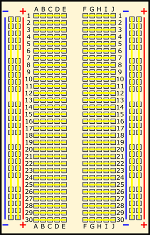
What we want to observe is the pins in the middle. We’ll refer to the A-J lines as “columns” and the 1-30 lines as “rows.” (A2 would be column A, row 2). Notice the yellow lines connecting everything row-wise? If we want to connect something in series, we would want to connect them using pins in the same row. That’s all we’ll need for the purposes of DAV. (For reference, connecting things across columns would be connecting them in parallel.)
For the buzzer, make sure when you wire it to one of the FPGA pins of your choice, you connect it across the row!
Remember to connect one side of the buzzer to ground! Refer to its datasheet to determine which side to connect to ground. (Or, if it's not polarized, simply connect either one.)
1.2 Buzzers and Frequencies
The buzzer just needs an oscillating signal to make noise - a clock, for example. Remember how all notes are frequencies? You can look up a note that you want your buzzer to buzz at and find the frequency it needs. You can then generate a clock at that frequency using your clock divider and pass that clock to the output pin, which will be wired to your buzzer!
2 An Alarming Rate
It’s time to get to the actual lab! In this lab, you’ll be making an alarm clock. The inputs will be:
- a start/stop button
- a reset button
- the switches
- the built in 50 MHz clock
The outputs will be the six seven-segment displays on the board and a buzzer. Two digits are the minutes, two digits are the seconds, and two digits are hundredths of a second.
For example, 103325 would be 10 minutes and 33.25 seconds. (Hint: This means that you’ll need digits in base 6 as well as base 10.)
The design will be as follows:
- When the start/stop button is pressed, the timer should toggle between running and being paused.
- Remember! Our buttons are active low – when they’re not pressed, their output is high.
- When running, the clock should be counting down, and this should show up on the display as well.
- When paused, the display should remain at whatever time the display showed when it was first paused.
- The rightmost switch will be a speed switch that, when enabled, runs the alarm clock down twice as fast.
- The remaining nine switches will be used to control the starting time on the clock when it’s being set.
- When the reset button is pressed, the timer should deactivate and return to the starting value as determined by the switches.
- The output digits should be displayed on the seven-segment displays, and you can simply modify your modules from lab 1.
- Note that unlike in lab 1, certain digits can only be from 0 to 5 instead of the usual 0 to 9 (so you’ll have to modify your code to reflect that).
- When the alarm clock runs down to zero, the buzzer should activate at an audible frequency of your choice.
So how do we get started?
2.1 The Block Diagram
This section does not require writing any code. Read it and move onto the next part before writing any Verilog.
We’re going to provide you with a block diagram for the alarm clock. A block diagram is essentially a bird’s-eye view of all the modules in the stopwatch and how they go together. This is a simplified version, i.e. not everything is connected up and the buzzer is missing – if it were complete, you wouldn’t have very much to figure out yourself :-)
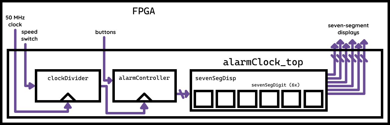
- Each rectangle is a “block,” or a module with the given name. (You can choose your own names if you’d like.)
- The wires coming from within
FPGAare pins on the FPGA that you will route into your top level module,alarmClock_top. - Ports coming out of the smaller modules will need to be declared as wires and driven by the output of that module. For example, you’ll need a wire driven by the output of
clockDividerthat gets routed as an input intoalarmController. - A little triangle at the bottom of a module indicates that the module is sequential and uses the wire going into the triangle as a clock. For example, our clock divider is clocked on the FPGA’s own 50 MHz clock pin.
- A wire with a line through it indicates that that wire is made up of many bits. These multi-bit wires are formally known as buses.
2.2 The Finite State Machine
It’s time to make a finite state machine of our own! Yay!
First, we have to design it. This entails drawing the diagram with the circles and arrows. We’ll give you a description of the states, their transitions, and how they affect the outputs; and it’ll be up to you to figure out how to put the pieces together.
Here are a few quick hints for you when you’re designing your FSM.
- There are three values in this system that will trigger state transitions: the pause/start button, the reset button, and the time remaining on the alarm clock. You do not need a state transition triggered by any other input.
- Remember the strategy we discussed in lecture for reading the edge of an external input, like a button or an external clock? You’ll need to apply that here!
Last note: FSMs are scary! If you need help or can’t figure out how to piece it all together, please reach out to us – we’re happy to provide a few more hints!
SET
- In this state, 9 switches (don’t include the clock speed switch!) can be used to manually adjust the time remaining on the clock.
- The switches can be treated as one 9-bit number, with the binary representation of the switches indicating the number of seconds (NOT the hundredths of a second).
- If the user presses the **pause/start button, **the alarm clock should start RUNning.
- If the user presses the reset button, nothing should happen, i.e. the alarm clock should stay in this state.
RUN
- During this state, changing the switches should not impact the timer.
- The time remaining should count down every second or half a second, depending on the speed of the alarm clock as indicated by the speed switch.
- Note that this doesn’t mean the speed switch has to be an input to the FSM! You can accomplish this just as easily by having the
- If the user presses the pause/start button, then the timer should be PAUSEd.
- If the user presses the reset button, the timer should be reSET.
- If the time remaining reaches zero, the alarm clock should start BEEPing.
PAUSE
- During this state, the timer should not count down, and the display should flash the paused time.
- It’s up to you what frequency the flash is, however, please make sure the flash is discernible.
- If the user presses the stop/start button, the timer should resume RUNning.
- If the user presses the reset button, the timer should be reSET.
BEEP
- During the BEEP state, the buzzer beeps, and the display flashes at 00:00:00 to show that the timer has finished.
- In the event that you are hearing-challenged like I (Claire) am, this buzzer is barely audible. You need to really lean close to hear it, and even then, I still couldn’t hear it :(
- If the user presses the **stop/start button, **nothing happens.
- If the user presses the reset** button,** the timer should be reSET.
Remember: For finite state machines, the next state should be computed combinationally based on the current state (and sometimes the inputs), but the actual state change event should be sequential.
3 It’s About Time
Now that you have the finite state machine drawn out and the buzzer set up, it’s time to code it! Refer to the block diagram in 2.1. You already made your clock divider and you have seven-segment digits from Lab 1. In this part of the lab, you need to write your top level module alarmClock_top – which merely declares input/output ports and wires the other modules together – and your alarmController. The alarmController, of course, will be your FSM module – you should write the Verilog code for your FSM as you designed it in section 2.
3.1 Implementing an FSM
Here’s a quick primer on how to implement an FSM in Verilog. The following code blocks are examples with arbitrary state transitions, state names, and outputs; only the overall code structure is relevant and not the values or names themselves.
Your module will need to have two always blocks: one sequential (clocked) and one combinational. In the sequential block, you should capture the edges of any unsynchronized values, set your outputs, and execute state transitions.
input button;
output reg [1:0] outVal;

reg [1:0] button_sr;
reg [1:0] currentState;
reg [1:0] nextState; // the next state to be assigned
reg [1:0] outVal_d;  // the next output value to be assigned

always @(posedge clk) begin
    /* shift the shift register left by 1 and
    store the current button value */
    button_sr <= { button_sr[0], button }

    /* state transition */
    currentState <= nextState;

    /* output assignment */
    outVal <= outVal_d;
end
In the combinational block, you determine the next state depending on your current state, your inputs, and any other values. You also determine the “next” output value to be assigned on the next clock cycle. Remember to use localparams to give your state values actual labels! It helps make your code more readable.
localparam STATE1 = 2'b00;
localparam STATE2 = 2'b01;
/* other states go here */

always_comb begin
    case (currentState)
        STATE1: begin
            /* remember that this won't be "assigned"
            until the sequential block executes on
            the clock edge! */

            /* if the button has a positive edge (i.e.
            it was just pressed, transition states */
            if (button_sr == 2'b01) begin
                nextState = STATE2;
                outVal_d = 2'b01;
            end else begin
                nextState = STATE1;
                outVal_d = 2'b11;
            end
        end
        /* other states go here */
    endcase
end
Just one more tip: for the display flashing, you don’t need a separate state or state machine (apart from BEEP)! Think about whether or not you could use bit tricks to override what the display is showing.
Happy coding, and don’t forget to pin plan!